16-bit Multicycle CPU on FPGA
✓ Completed

Designed and implemented a fully functional 16-bit multicycle CPU from scratch in Verilog HDL, synthesised and deployed on an Intel DE10-Lite FPGA board. The processor executes a custom instruction set architecture (ISA) and displays computed results in real time on the board's seven-segment HEX displays and LEDs. This project demonstrates end-to-end digital design — from individual logic components through to a working stored-program computer running on real hardware.
Built as part of Monash University ECE2072 in collaboration with Daniel Mathew. The design is fully modular, with every component — ALU, registers, control FSM, sign extender, clock divider, and display driver — independently implemented and tested before integration.
Key Features
- 16-bit datapath with 8 general-purpose registers (R0–R7)
- Custom 9-bit ISA — arithmetic, logic, immediate, shift, branch, and display instructions
- Multicycle execution via a 4-state tick FSM (fetch → decode → execute → write-back)
- Branch support (
bez) enabling conditional loops and Turing-complete programs
- Integrated instruction memory via Intel ROM IP (altsyncram), loaded from a
.mifprogram file - Real-time output — signed decimal results shown across five 7-segment HEX displays
- Observable execution — 50 MHz clock divided to 10 Hz for step-by-step debugging
- Fully modular RTL design — all components independently parameterised and reusable
Instruction Set Architecture
The CPU uses a 9-bit fixed-width instruction encoding: bits [8:6] carry the opcode,
[5:3] the destination register Rx, and [2:0] the source register Ry or an immediate value.
Immediates are 9-bit two's complement values, sign-extended to 16 bits before use.
| Opcode | Mnemonic | Operation |
|---|---|---|
000 | display Rx | Output Rx to HEX display |
001 | add Rx, Ry | Rx ← Rx + Ry |
010 | addi Rx, imm | Rx ← Rx + sign_extend(imm) |
011 | sub Rx, Ry | Rx ← Rx − Ry |
100 | mul Rx, Ry | Rx ← Rx × Ry |
101 | ssi Rx, imm | Rx ← Rx shift sign_extend(imm) |
110 | bez Rx, imm | PC ← PC + imm if Rx == 0 |
111 | movi Rx, imm | Rx ← sign_extend(imm) |
Hardware Architecture
Datapath
The core datapath is built around a single shared 16-bit internal bus driven by a 10-to-1 multiplexer. Sources include the eight general-purpose registers, the ALU output buffer (G), and the sign-extended immediate from the instruction register. Four additional special-purpose registers handle intermediate pipeline state:
- IR — Instruction Register, latches the current 9-bit instruction from ROM
- A — Accumulator, holds the first ALU operand between ticks
- G — ALU output buffer, holds the computed result before write-back
- H — Display latch, drives the HEX output independently of ongoing computation
The ALU supports four operations: addition, subtraction, multiplication, and a signed bidirectional shift (positive shift amount = left shift, negative = arithmetic right shift).
Control Unit
A purely combinational control unit decodes the opcode in the instruction register alongside the current tick FSM state to generate every datapath control signal — register write enables, bus select, ALU opcode, and program counter update logic. This clean separation of control and datapath reflects a standard hardwired control unit architecture.
Instruction Memory
A 65536 × 9-bit synchronous ROM (Intel altsyncram IP) stores the program.
Instructions are loaded at synthesis time from a Memory Initialisation File (.mif),
with the 16-bit Program Counter used directly as the ROM address.
Display System
A Double Dabble (shift-and-add-3) BCD conversion module converts the 16-bit signed result into individual decimal digits. Five 7-segment decoders drive HEX0–HEX4, showing values from −32,768 to +32,767 with sign indication. HEX5 shows the current tick FSM state for real-time hardware debugging, and LEDR[9:0] mirrors the lower 10 bits of the internal bus.
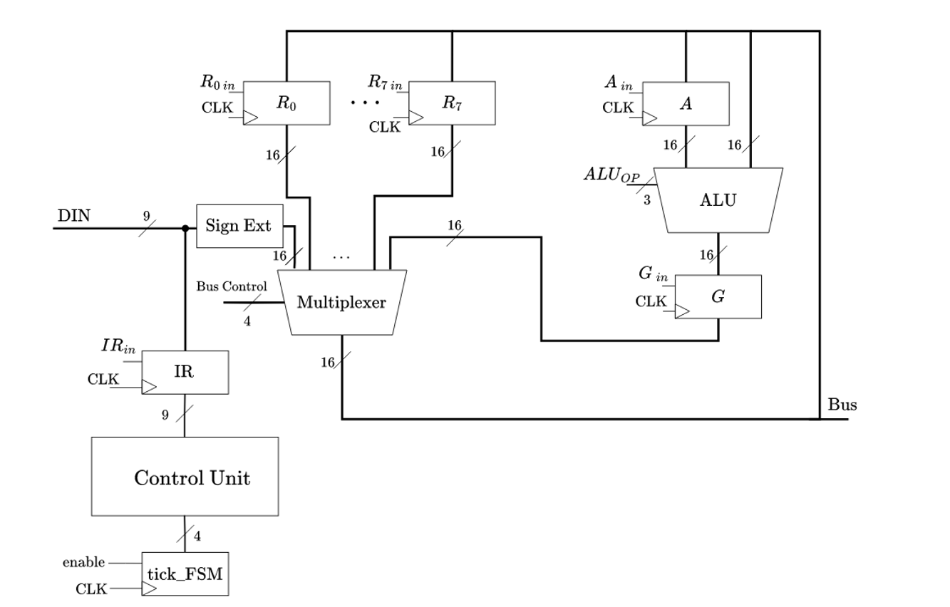
Figure 1: Internal CPU architecture and datapath
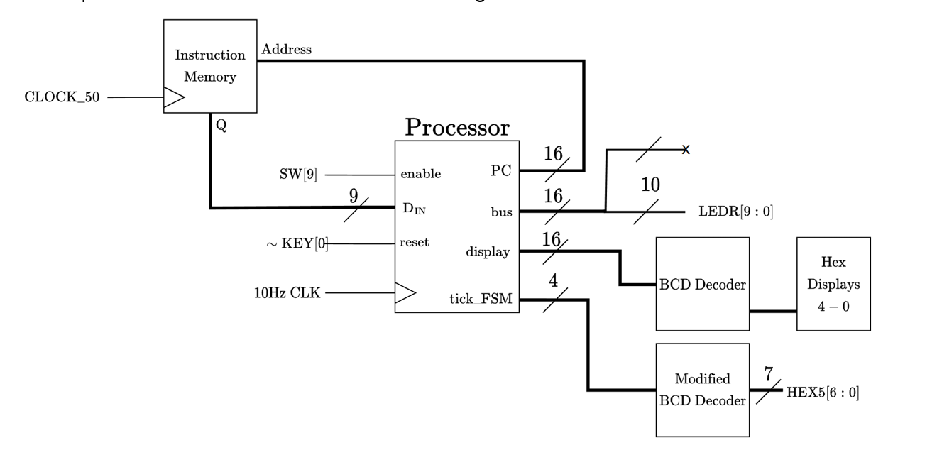
Figure 2: CPU connections to ROM, HEX displays, and peripherals
Module Breakdown
| File | Module | Description |
|---|---|---|
components.v | register_n | Parameterised N-bit register with synchronous reset and write enable |
components.v | ALU | 4-operation ALU: add, subtract, multiply, signed shift |
components.v | multiplexer | 10-to-1 16-bit bus multiplexer |
components.v | tick_FSM | 4-state one-hot instruction cycle FSM |
components.v | sign_extend | 9-bit to 16-bit two's complement sign extender |
proc_memory.v | proc_memory | Full CPU core — integrates ROM, PC, datapath, and control unit |
proc_memory_inst.v | proc_memory_inst | Top-level FPGA instantiation with board I/O pin mapping |
BCD_decoder.v | BCD_decoder | Double Dabble binary-to-BCD converter with 7-segment driver |
rom.v | rom | Intel altsyncram ROM IP wrapper |
tenHz.v | tenHz | 50 MHz → 10 Hz clock divider (counter-based) |
Skills Demonstrated
- RTL design and Verilog HDL coding
- CPU microarchitecture: datapath, control unit, multicycle pipeline
- FPGA synthesis and board deployment with Intel Quartus Prime
- Finite State Machine (FSM) design
- Intel FPGA IP core integration (altsyncram, LPM_DIVIDE)
- Binary arithmetic: two's complement, sign extension, BCD conversion
- Hardware debugging with LEDs and seven-segment displays
- Modular design and component-level verification